
After several years of being department chair, I am very much enjoying being on research leave this year. A research leave is an opportunity for Wooster faculty to take a semester or a year just to focus on our research, without any teaching, committee work, or other kinds of administrative work. It’s a time to meet new people, get new ideas, and learn new things. I have two major research trips planned this year to expand my perspectives, and to develop some collaborations.
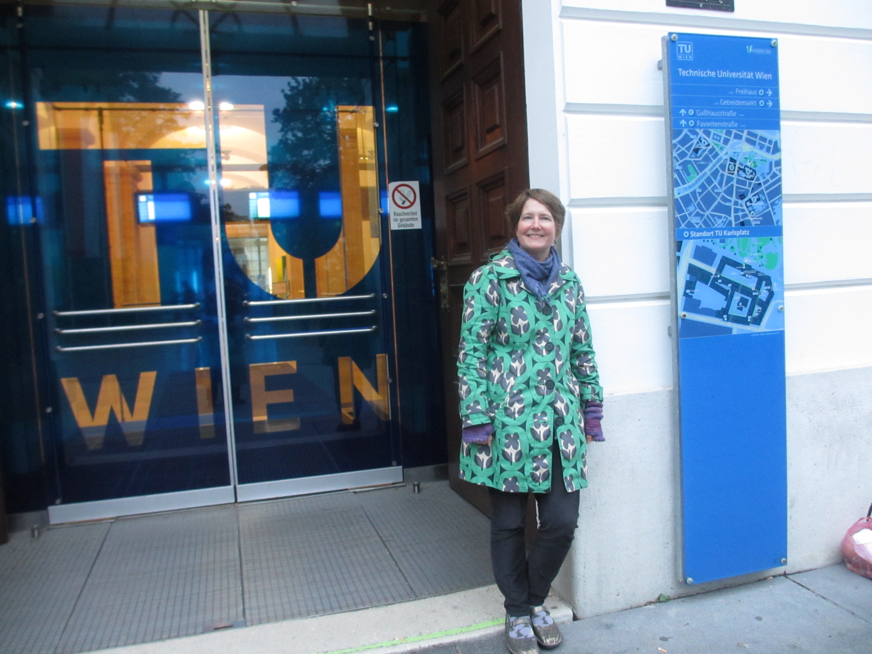
I recently returned from the first trip — which was to visit my colleague Dr. Jürgen Smoliner at the Institut für Festkörperelektronik of the Technische Universität Wien, or in other words, the Institute for Solid State Electronics at the Vienna University of Technology. I first visited Dr. Smoliner on my last leave in 2012, when I wanted to get better at the technique of ballistic electron emission microscopy, and it has become a great collaboration for both of us.
As an American, one of the things that I most love about visiting Vienna is the history. (I’ll get more into this in a later post, about not doing physics in Vienna!) For example, Christian Doppler of the famous Doppler effect was a graduate of TU-Wien!
On this visit, though, there was no Doppler effect involved. We were doing ballistic electron emission microscopy (BEEM), which is a variation of scanning tunneling microscopy (STM) where there is a very thin additional contact on top of the sample of interest. Ultimately, the plan was to investigate nickel on gallium arsenide, but there were some technical challenges, so we spent most of the time with the standard test sample of gold on gallium arsenide.
To make the samples, we need to create a layer of gold that is around 8 nm thick — that is, extremely thin! The gallium arsenide must be absolutely clean first, so it is dipped in hydrochloric acid, and then placed into the vacuum chamber where the gold will be deposited. We used a thermal evaporation system for the gold, which (funnily enough) is the very first thing I ever learned to do in graduate school! (Thank you, Dr. Briscoe!) Unlike my work in grad school, though, we did all of this sample processing in a clean room.
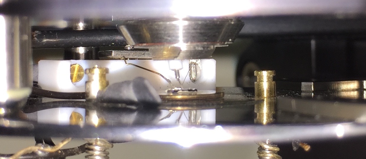
Once the gold layer has been evaporated onto the gallium arsenide, we could make the electrical connections and actually begin making measurements. In BEEM, we need two electrical connections to the sample — one connection to that thin gold layer, and one connection to the gallium arsenide itself. In the top view image, you can see the thicker wire (with a little indium gooped on the end to make it sticky) connecting to the top of the sample. It’s actually touching one of the gold lines on the sample, but that wasn’t visible in the picture. The thinner gold wire was tucked underneath the round mounting disk in this picture, but for our actual measurements it was moved to the top of the sample. I took this picture through the eyepiece of an ordinary optical microscope — the coppery-colored disk that the sample is sitting on is actually about 1 cm in diameter.

In the side view picture below, you can see the sample once it was mounted in the STM. If you look closely, you can see that same thick gold wire, the thin gold wire, and also the STM tip coming down to image the sample. I was surprised to get this good a picture from an iPhone! (Thank you, optical physicists who work for Apple!)
So, like all experimental physics, it takes a good bit of time to get to this point — sample prepared, system working– and then you can actually hope that it will all keep working long enough to get some good data! We were able to get good data for the gold on gallium arsenide sample, so that was a success! Also, I needed to test whether my home-built BEEM amplifier was still working, and fortunately, found out that it was. (There’s a long back story there — short version is that the BEEM current we measure is only on the order of picoamps, so we need a very sensitive, low noise amplifier in order to make this signal measurable. This exact configuration is not something that is available commercially, so we built it ourselves a few years ago, but had been having trouble and were not sure whether something had happened to the amplifier. So, I took it along to check out.)
While at TU-Wien, I also taught a brief graduate seminar on BEEM of nanostructures (aka, Ballistische Elektronenmikroskopie auf Nanostrukturen). It was fun teaching at a very different level than I am used to. And, one of the students taking the course suggested that BEEM might be a good tool to look at some of the samples that his group studies, so it could very well end up in a new collaboration!
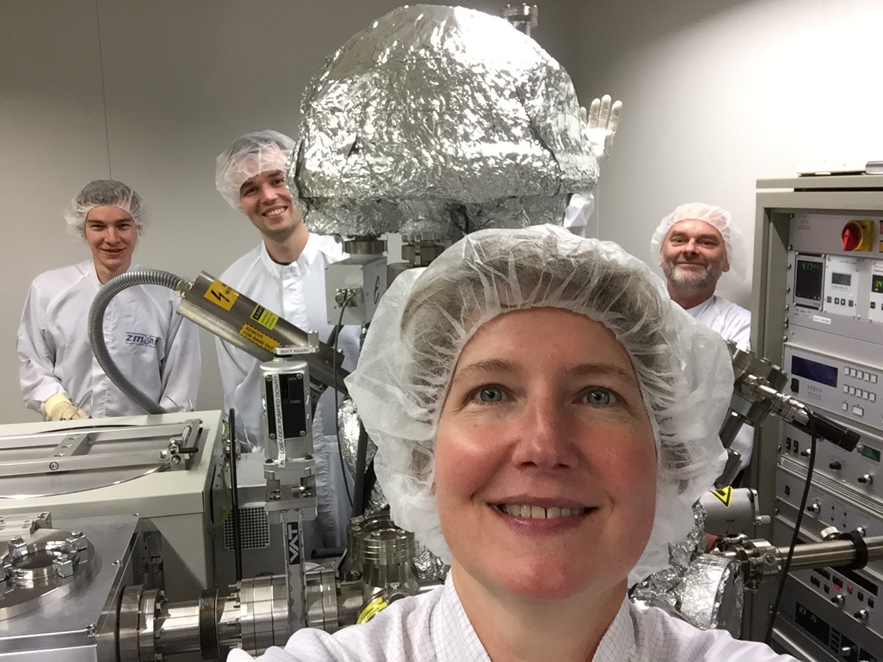
The people that I was working with are all in the ZMNS at TU-Wien, which is the Center for Micro and Nano Structures. The university is currently building a new building (actually, starting with the base of an extremely *old* building) for ZMNS which will have a new and larger clean room. So, I am looking forward to checking that out on my next visit to Vienna!
Stay tuned for posts on what else there is to do in Vienna besides physics!
Thanks, Mark! I enjoy reading your posts as well.